- This web page was last updated on
Wed, 2014 Mar 26 @ 1455 hours
- Questions about this page?
Contact us by email.
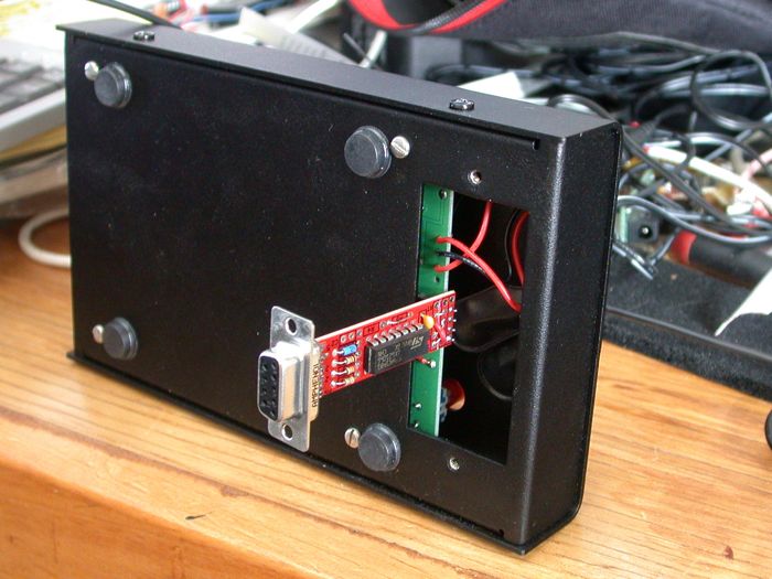
The AMQRP NUE-PSK Modem is field re-programmable. The port is TTL/CMOS and requires a level shift/inverter.
The P4B Kit is an RS232 to TTL level shifter can be easily adapted to do the job at much less than half the cost of other solutions
I also stock a USB to TTL serial adapter, the USB-BUB(NP) that has a USB mini-B female receptacle and terminates in a 6 pin molex KK on the other end.
I sell it for use programming my Arduino/Freeduino boards. It is an exact functional equivalent to the FTDI cable I used to sell,
only $5 less expensive. Using a small generalized adapter board it can be used to program the NUE-PSK. Simply unplug the adapter board
and it can be used for many other things.
I strongly suggest visiting the FTDI site and downloading the
most recent drivers. Here is the link to the FTDI Drivers Page
| P4B - NP |
USB-BUB(NP) |
|
|
| P4B - bare PCBs |
Qty = 1
$2
|
Qty = 3
$5
0 |
Qty = 5
$8
|
Qty = 10
$15
|
| P4B - TTL-to-RS232 adapter |
Kit - Qty = 1
$5
|
Kit - Qty = 3
|
|
|
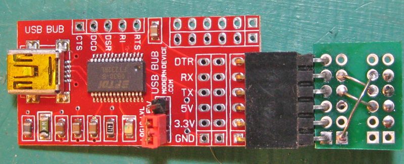
FTDI USB-BUB Cable
w/NUE-PSK Adapter |
This is the FTDI based, USB-BUB USB to TTL serial adapter. It comes with a USB A to mini-B cable.
I supply a pre-wired adapter board which attaches internal programming port of the NUE-PSK modem. You may
download the manual here.
This cable can be quite useful for other projects.
|
$19
|
|
|
P4B - Assembly for NUE-PSK Modem
- Simple schematic and pictorial available.
- Complete P3/P4 manual available.
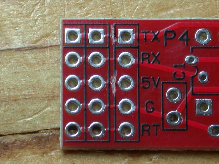
- (steps 3 through 10 apply to both the P4 and the P4B) Holding the board with the solder tabs towards you, from right to left insert the three resistors; 180 ohms (brown-gray-brown),
22 Kohms (red-red-orange, 10 Kohms (brown-black-orange), then the Diode (black band towards chip)
- solder and clip these leads off
- We will not use the hexgate for the reset circuit. But we must either ground or pull up its input line to prevent the gate from
randomly oscillating. So, along the left edge where you would place C2, R4, and R5. Leave out C2 ("104") and R4 (10K). Insert
a clipped resistor lead as a jumper in place of R5 (10K), effectively grounding the gate input. Place C1 0.1 uF ("104"), solder,
and clip excess leads
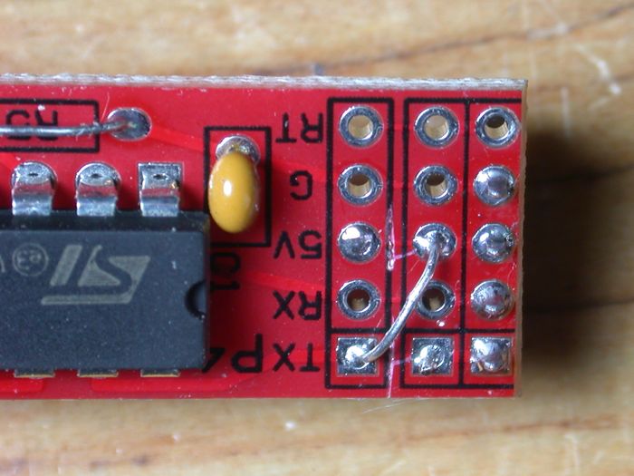
- Carefully lay the chip on its side and push it evenly from both sides so the legs are more perpedicular to the chip rather than splayed outward
as it comes from the factory. Then turn the chip on its other side and do the same
- Align the chip with its notch towards the three rows of 5 holes end. (if you hold the PCB so you can read the words "Wulfden/ModernDevice", then
the writing on the chip will be upside down). Now carefully insert the chip into the 14 holes.
- check that all pins are through their respective holes, bend a two pins over at diagonally opposite points to hold the chip in place while you solder.
- Solder and clip these leads.
- Push the DB9 plug pins over the edge of the board. With some of these connectors they do not line up absolutely perfectly but well enough that they
can be soldered on without making any unwanted solder bridges.
- (for P4B only) The P4B will require NO cuts. The row and pin references are the same. See picture
- Insert jumper wire to connect Pin 1/Row 1 - GND to Pin 5/Row 2
- Insert jumper wire to connect Pin 5/Row 1 - RX to Pin 4/Row 2
- Insert jumper wire to connect Pin 4/Row 1 - TX to Pin 3/Row 2
- Insert jumper wire to connect Pin 3/Row 1 - +5 to Pin 2/Row 2
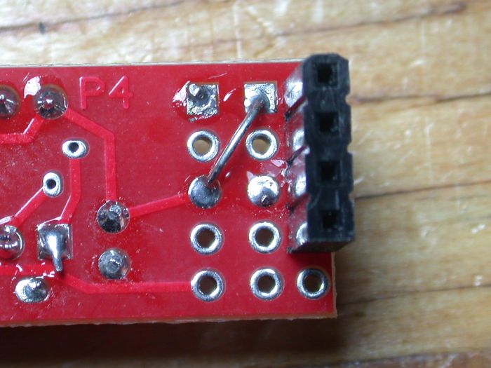
- (for P4B conly)Insert the 4 pin socket header facing down, pins up though pcb into the row three holes for pins 2-5
(centering it)
and solder on the top component side, make sure its perpendicular to the plane of the pcb,
|